
The Relentless Pursuit of Engineering Perfection
Supremacy is not purchased; it is engineered. Raghu Panicker, CEO of Kaynes Semicon, argues that the true test of our ambition lies in mastering the unforgiving physics of zero defects.
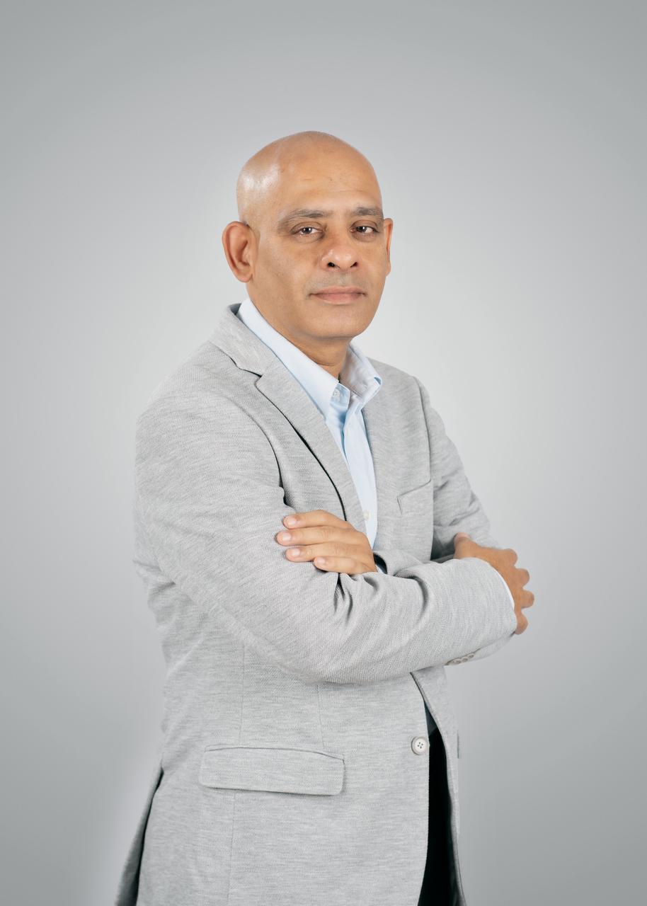
Raghu Panicker
The thrilling race for India's semiconductor sovereignty requires operational excellence. Economic stakes are high: the domestic market, worth over $41 billion, is expected to grow 19% to $109 billion by 2030. National investment in ten packaging and fabrication projects has accelerated this historic opportunity.
But turning this momentum into technological autonomy requires capital and high-quality standards. The zero-defect mandate depends solely on outsourced semiconductor assembly and test (OSAT). Perfect, world-class execution across materials, infrastructure, and human capital is now the main challenge, not investment.
In this high-stakes environment, the perspective of key industry figures is vital. Raghu Panicker identifies the "Zero Defect" mandate as the industry's great filter. His vision extends beyond simply building factories; it encompasses the development of a self-sufficient ecosystem capable of surviving the unforgiving physics of advanced packaging, propelling India to the forefront of next-generation packaging technologies.
Built to Endure
The pursuit of global yield rates is the ultimate test of an OSAT ecosystem. As India embraces advanced packaging methods essential for the next generation of 7nm and 5nm process nodes, the technical complexity increases exponentially. Miniaturised computing packages, which tightly integrate multiple specialised chips for logic, memory, and functions into a single unit, quietly undermine long-term reliability.
Such a challenge stems from the inherent friction created when dissimilar materials, such as rigid silicon and flexible protective polymers (the soft side of the chip), are tightly bonded together. When exposed to the intense, repeated heat and cooling cycles of real-world operation—as in a car engine or a high-powered AI data centre—these materials expand at different rates. This is the nightmare scenario: a chip that passes the factory test but fails in the field.
To fix this, Panicker advocates for urgent funding in material science. India's quality manufacturing must be founded on proprietary polymer science rather than on borrowed process optimisation. "We must own the chemistry of the adhesives and underfills that hold the package together rather than on borrowed process optimisation,". He argues that Indian research and development should focus on creating and standardising high-reliability and low-stress polymeric materials.
Intelligence over Inspection
Data drives efficiency in an industry where nanometre precision and tight margins are paramount. Traditional controls have proven too slow for the demands of modern scaling. The global market for digital twin technology is experiencing significant growth, projected to expand at a compound annual growth rate (CAGR) of approximately 48%. This transformation represents a shift from reactive control to proactive, intelligent governance.
In an industry where margins are measured in nanometres, traditional quality control is too slow. Panicker highlights the "highest immediate return" investment: AI-driven predictive manufacturing. He asserts that this optimal return stems from the strategic integration of Predictive Yield Optimisation (PYO) and Virtual Metrology (VM). This approach leverages machine learning to swiftly analyse vast amounts of real-time sensor data on the factory floor, enabling the prediction of potential defects.
"By merging PYO with predictive maintenance—which has the potential to reduce unexpected downtime by 20%—we address the dual need for consistent quality and stable production," Panicker elaborates. "Moreover, our attention must be directed towards advanced digital twin models that utilise sophisticated computational techniques. This method encompasses the application of computational fluid dynamics (CFD), which simulates heat transfer within the packaged chip, and finite element analysis."
Securing Global Trust
India's commitment to the semiconductor ecosystem is substantial. Yet accessing the global market, particularly high-reliability sectors, demands immediate, ironclad trust. Securing certification from a major international Tier-1 customer involves a gruelling process of deep quality audits, detailed documentation (like PFMEA), and the rigorous production part approval process (PPAP).
To overcome the perception of being a nascent ecosystem, India needs a single mechanism to validate its quality baseline. "The policy mechanism most needed to rapidly build global trust and facilitate certification for all Indian OSAT players is the establishment of a National Consortium Quality Board (NCQB)," Panicker argues. This industry-led board will harmonise all quality documentation and enforce compliance with global standards by issuing a formal, globally recognised process maturity endorsement.
Collective investment in capital-intensive resources is required to move to advanced chip stacking, which is vital for AI and high-performance applications. High-end metrology tools—the specialised machines necessary for the non-destructive inspection of ultra-fine-pitch microbumps and verification of precision assemblies—are expensive for the new entrants. "To enable the ecosystem to successfully implement advanced packaging, the critical shared resource needing immediate collective investment is a National Advanced Packaging Metrology Center (NAPMC)."
Mastering the Execution
The strategic localisation of the semiconductor industry's supply chain is crucial for self-sufficiency. Although securing silicon wafers remains a long-term goal, there is presently a promising opportunity within the field of speciality materials. Panicker observes that semiconductor-grade encapsulation materials (moulding compounds) are among the most vital input materials that could be fully localised in India over the next two to three years. India's well-established chemical industry provides a foundation for this capability.
While the ISM provides 50% financial assistance for capital expenditures, the real need lies in policy support that goes beyond monetary aid. Panicker advocates for the implementation of guaranteed consumption agreements (GCAs). He states, "It is imperative that all subsidised OSAT units, such as those supported by Micron, Tata, and CG Power, are mandated to use a specified proportion of locally approved encapsulation materials." This policy reduces the risk linked to the material transition.
Additionally, the concluding phase of testing often emerges as a considerable bottleneck. Currently, the Indian ecosystem does not possess adequate specialised testing equipment (referred to as Automatic Test Equipment, or ATE), which is necessary for high-frequency, advanced devices crucial for 5G, electric vehicles, and AI applications. Although the Design Linked Incentive (DLI) scheme promotes indigenous chip designs, this limitation hampers their validation procedures.
Panicker underscores that the development of national advanced testing centres (NATCs) must be a central priority of the nation's investment policies. Consolidating specialised ATEs in shared facilities reduces the financial burden on individual companies. "We must promptly establish and execute standardised testing protocols to ensure that this process complies with international standards," he maintains.
Finally, the entire endeavour rests on human capital. India needs 85,000 skilled engineers by 2027 to meet the surging demand in the electronics sector. The most challenging specialised skill to instill in entry-level staff is not technical knowledge but operational discipline—static-safe precision handling (ESD-compliant microhandling). This skill demands continuous, non-negotiable adherence to protocol. "To standardise this critical procedure and overcome cultural inertia, we need rigorous training and certification programs."
To maintain this highly specialised workforce and ensure permanent expertise, two structural solutions are proposed: to prevent the operational wisdom brought by expat experts from departing, Panicker calls for the India Semiconductor Technology Transfer Fellowship (ISTTF). "This program should require that expats clearly document important operational steps and the key principles of a zero-defect culture in official, localised training manuals." He explains that this process transforms tacit knowledge into permanent institutional wisdom.
Panicker calls for the National Semiconductor Engineering Accreditation Framework (NSEAF) to support the highly trained technicians whose mastery of cleanroom procedures is vital. This step-by-step accreditation system, which relies on proven skills, needs to establish official partnerships with state technical universities to award academic credits for specialised cleanroom experiences. This national recognition elevates the technician's professional status and provides a clear career path.
Solutions Spotlight
- •The Trust Engine: Establish a National Consortium Quality Board (NCQB) to issue global-standard "Process Maturity Endorsements," accelerating vendor qualification.
- •The Shared Eye: Create a National Advanced Packaging Metrology Center (NAPMC) to provide startups access to ultra-expensive inspection tools without the CapEx burden.
- •The Chemistry First Policy: Fund proprietary polymer science R&D. We cannot rely on imported glues; we must own the materials that hold the chip together.
Strategy Note
Panicker's masterstroke is the GCA (Guaranteed Consumption Agreement). By legally forcing PLI beneficiaries to source a percentage of materials (like moulding compounds) locally, he creates an instant, guaranteed market for Indian chemical companies, removing the risk of entry.
Key Takeaways
- The Thermal Timebomb: The biggest risk isn't electrical; it's mechanical. Thermal mismatch between chip and package is the silent killer we must solve with material science.
- Predict, Don't Inspect: Traditional QC is dead. The future is Virtual Metrology and Digital Twins that predict failures before they occur.
- Tacit Knowledge: We must capture the muscle memory of expat experts. The India Semiconductor Technology Transfer Fellowship should mandate that expats document their unwritten operational wisdom into permanent manuals.