India’s semiconductor story has been looking at the wrong surface.
The chip carries the brand. The fab carries the national ambition. The substrate carries the system.
A chip can be designed well. A wafer can be fabricated well. But the system only works when the hidden layers beneath the chip can carry power, signal, heat, and density without failure. That hidden layer is where advanced semiconductor manufacturing becomes physical. A flawless chip attached to a deficient substrate is expensive, non-functional silicon.
That is where the Odisha–Intel–3DGS pact enters the semiconductor argument.
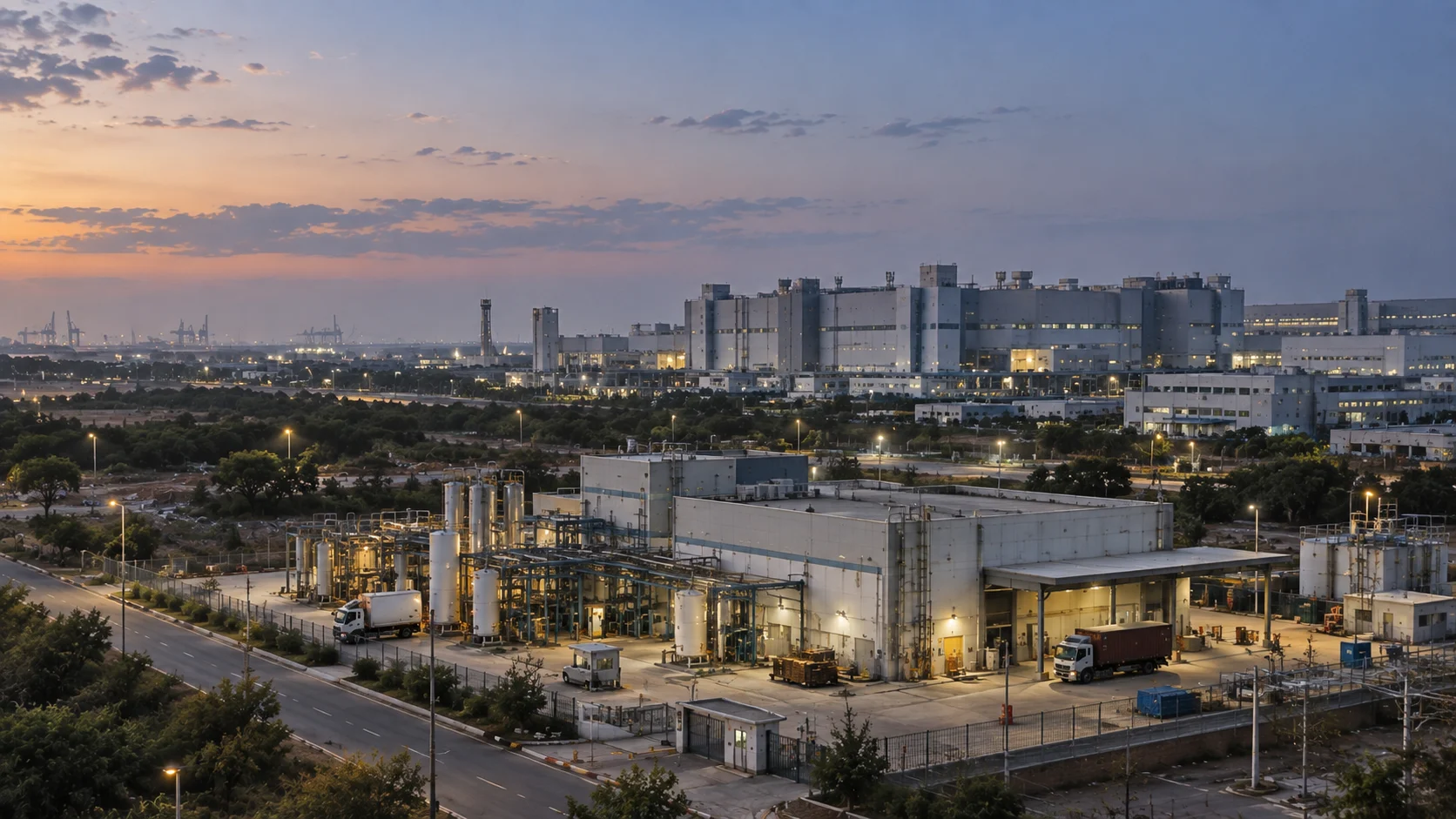
The Odisha–Intel–3DGS agreement points India toward a proposed advanced packaging glass-core substrate manufacturing facility in the Bhubaneswar–Khurda region. The MoU was signed on May 29, 2026. The proposed investment, reported at about $3.3 billion, gives the pact scale. Intel’s role is expected to include technology know-how, process expertise, licensing support, quality systems, and workforce capability building. The real value lies in the manufacturing layer it targets.
For years, India’s semiconductor ambition has been judged through the glamour of wafer fabrication. The question matters, but it is incomplete. A semiconductor economy is not built by one fab alone. It is built by the stack around it.
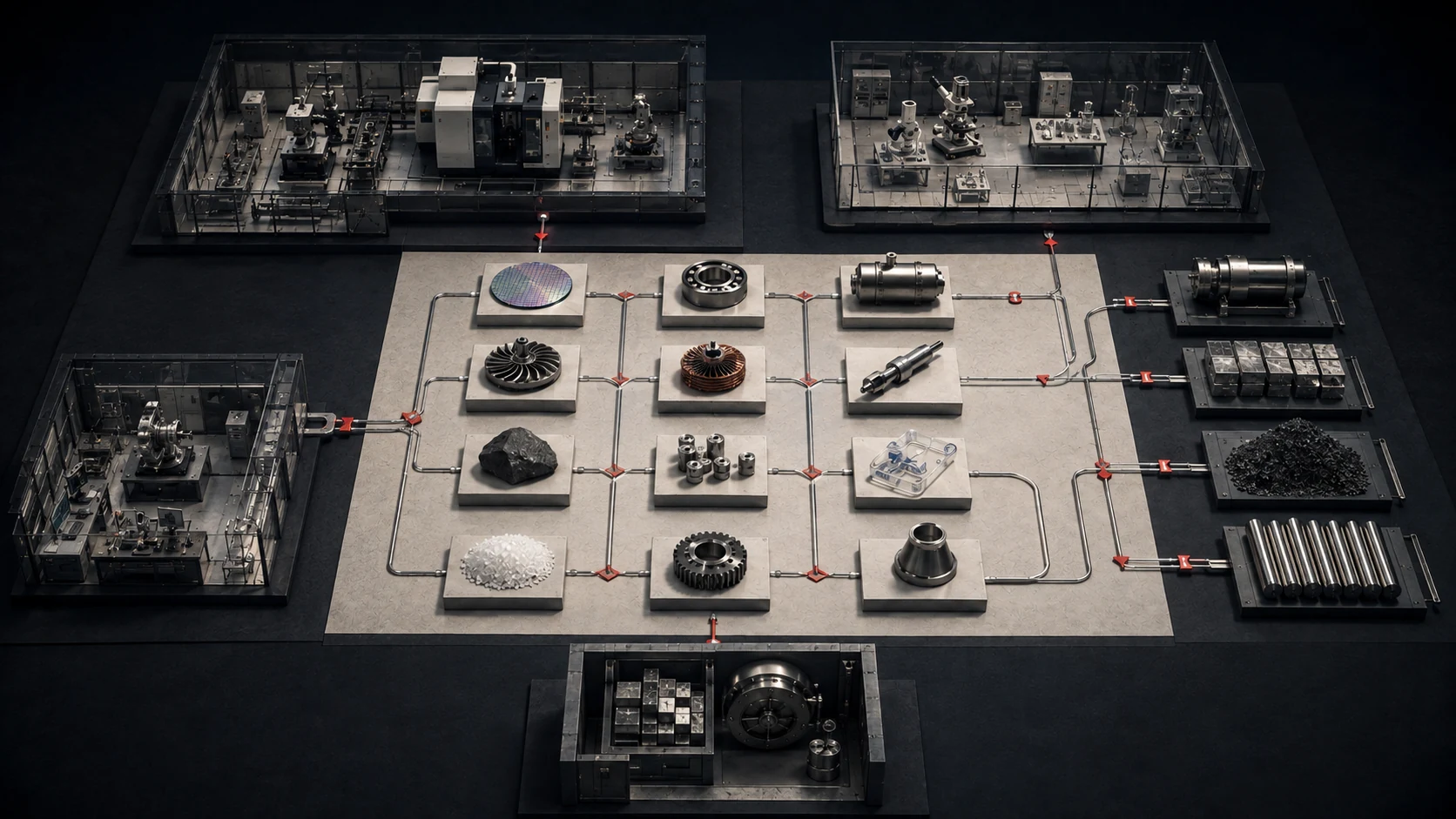
The Semiconductor Control Stack
Miss one layer, and value leaks out of the country.
India has already learned this lesson in electronics. Assembly can create scale. It can create jobs. It can build market access. But assembly isolated from the component ecosystem creates scale without deep control. The deeper value sits in design, components, materials, tooling, process knowledge, and supplier qualification.
Semiconductors make that lesson sharper.
The substrate is not glamorous. It rarely appears in public conversation. It sits beneath the chip, connecting the die to the package and the board. But in advanced semiconductor systems, that layer becomes a gate. It affects signal movement, power delivery, thermal stability, density, reliability, and packaging complexity. In plain terms, the chip can be brilliant and the system can still fail if the substrate cannot support it.
The semiconductor race has moved beyond the transistor alone. Advanced packaging, chiplets, high-density interconnects, and thermal management now decide how much performance a system can actually deliver. The contest is no longer only about shrinking the node. It is about connecting chips faster, moving power cleaner, controlling heat better, and holding reliability at scale. Substrate capability sits directly inside that contest.
A glass-core substrate facility brings India closer to advanced packaging and forces demand for engineers who understand difficult material processes. It also shortens the distance between substrate supply and packaging demand, allowing customers to test India beyond final assembly.
The transition India is attempting is from chip presence to chip-stack control.
Odisha’s role is not incidental.
For decades, the state has been read through minerals, metals, ports, power, and heavy industry. The substrate facility changes the test. Odisha’s task is conversion: from heavy industry to precision manufacturing.
Minerals, metals, ports, and power gave the state industrial weight. Semiconductor substrates will test whether that weight can become cleanroom reliability, trained labour, water security, logistics discipline, and administrative speed.
High-tech manufacturing rewards repeatability. Semiconductor facilities are built on unforgiving routines: contamination control, equipment uptime, process recipes, supplier qualification, metrology, maintenance, audits, and yield learning. A plant becomes strategic only when it can produce repeatedly, qualify globally, and survive customer scrutiny.
The pact opens the door. Execution decides whether the door becomes a corridor.
India’s semiconductor mission must therefore resist the comfort of trophy language. One fab will not build the ecosystem. One packaging unit will not complete the chain. One substrate facility will not create sovereignty. The stack has to be built as an industrial system.
The Dependency Chain
Wafer fabrication needs suppliers.
Packaging needs substrates.
Substrates need materials.
Materials need process control.
Process control needs equipment, engineers, chemicals, gases, metrology, and maintenance depth.
The real industrial work begins there.
If the Odisha facility moves from agreement to production, India gains more than capacity. It gains proximity between substrate supply and packaging demand while developing a skill base in an invisible but critical manufacturing layer. This gives semiconductor customers a reason to place deeper trust in India’s process capability. Most importantly, it moves the country into a layer that final assembly depends on.
Semiconductor sovereignty is not declared. It is manufactured through layer control.
Solutions Spotlight
To convert the pact into capability, Odisha must protect the facility from the ordinary friction of Indian industrial execution. The single window has to become a technical command window: clearances, utilities, environmental compliance, and supplier onboarding under one accountable authority.
The second requirement is shared industrial infrastructure. A metrology and reliability lab near the cluster would help domestic suppliers qualify faster and reduce dependence on distant validation loops.
Strategy Note
The industrial strategy must bring substrate production closer to India’s emerging Outsourced Semiconductor Assembly and Test (OSAT) capacity. The stack has to tighten physically before it can deepen economically.
That also requires a talent pipeline. Regional technical institutions should run dedicated tracks in semiconductor packaging, cleanroom operations, and metrology to build operators and technicians for the layer India is trying to enter.
Execution Test
The real test is not the announcement alone. It is whether the facility gets built, reaches process stability, supplier qualification, yield economics, and customer trust.
The chip remains the visible prize.
The substrate is the silent gate.
In the next phase of semiconductor manufacturing, the gate will decide who controls the stack.
Rishi Vora
Editor & Publisher, India Front
Rishi Vora is the Editor and Publisher of India Front, India’s premier thought-leadership magazine. He writes on governance, economic policy, and India’s strategic position in the global order.